-
ÜrünlerÜrünler
-
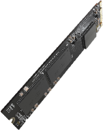
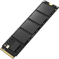
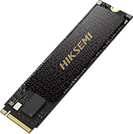
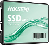
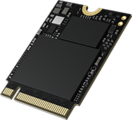
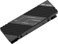
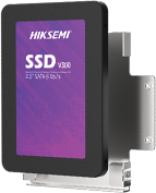
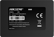
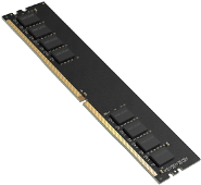
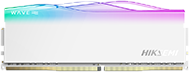
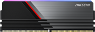
Katı Hal Sürücüsü
-
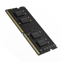
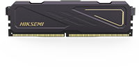
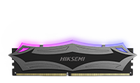
Hafıza
-
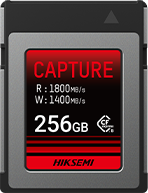
Hafıza Kartı
-
Harici depolama
-
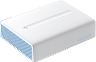
NAS
-
Aksesuarlar
-
Gömülü Depolama
-
-
Şirket
-
Çözümler
To appreciate the , compare it to similar models:
Before the CPU can transition to an active state, the motherboard must establish its baseline low-dropout (LDO) and pulse-width modulation (PWM) voltage lines. The top schematic level defines these primary rails:
Right next to the SoC, the top layer features , arranged horizontally or staggered to maximize signal integrity on the multi-layer PCB. 2. DC-In and Primary Power Generation Stage lad402p schematic top
Enters from the DC jack. It passes through the input protection MOSFETs ( PQ1 and PQ2 ) controlled by the charging IC.
Review the layout file to identify which branch circuits attach directly to the shorted plane. To appreciate the , compare it to similar
Usually an ENE KB9022Q. This chip manages the keyboard matrix, power-on sequence, thermal monitoring, and battery communication.
Need help identifying component labeled "LAD402P" (or similar) DC-In and Primary Power Generation Stage Enters from
LAD402P Schematic Top Layer: Complete Repair & Architecture Guide
Welcome to visit our website! So far, this website does not use any cookies. Through this website you will learn about our products, company profile, mission and value, etc.